At Angstrom Advanced our goal is to provide our customers with the best products with highest standard of service at cost efficient pricing.
Angstrom Advanced Inc. designs, manufactures and supplies a wide variety of atomic force, scanning probe, scanning electron, and lateral force microscopes for academic and laboratory fields. Our microscopes have been delivered to many renowned organizations world wide.
Angstrom Advanced has continuously innovated, improved and promoted its cutting-edge technology in atomic force microscopy. We have won the "Best of Boston" award in scientific instruments for four years running, and are on track to win it again in 2014.
The Angstrom Advanced microscope lineup types:
- Atomic Force Microscopy (AFM)
- Scanning Probe Microscopy (SPM)
- Scanning Electron Microscopy (SEM)
- Lateral Force Microscopy (LFM)
- Combined microscope systems
Be sure to check our website for the latest product updates and news. To learn more about our atomic force microscope equipment and technology, visit our corporate website at www.angstrom-advanced.com.
The AFM consists of a cantilever with a sharp tip (probe) at its end that is used to scan the specimen surface. The cantilever is a silicon or silicon nitride with a tip radius of curvature on the order of nanometers. When the tip is brought into proximity of a sample surface, forces between the tip and the sample lead to a deflection of the cantilever according to Hooke's law. Depending on the situation, forces that are measured in AFM include mechanical contact force, van der Waals forces, capillary forces, chemical bonding, electrostatic forces, magnetic forces, Casimir forces, solvation forces, etc. Along with force, additional quantities may simultaneously be measured through the use of specialized types of probe. Typically, the deflection is measured using a laser spot reflected from the top surface of the cantilever into an array of photodiodes. Other methods that are used include optical interferometry, capacitive sensing or piezoresistive AFM cantilevers. These cantilevers are fabricated with piezoresistive elements that act as a strain gauge. Using a Wheatstone bridge, strain in the AFM cantilever due to deflection can be measured, but this method is not as sensitive as laser deflection or interferometry.
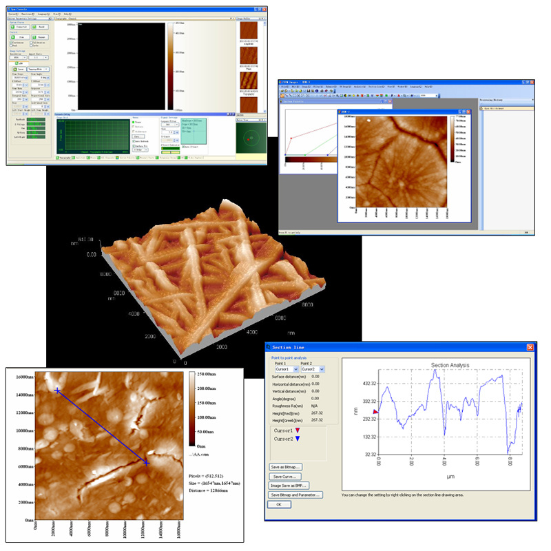
Atomic force microscope topographical scan of a glass surface. The micro and nano-scale features of the glass can be observed, portraying the roughness of the material. The image space is (x,y,z) = (20um x 20um x 420nm).If the tip was scanned at a constant height, a risk would exist that the tip collides with the surface, causing damage. The feedback mechanism is employed to adjust the tip-to-sample distance to maintain a constant force between the tip and the sample. The sample is mounted on a piezoelectric tube, that can move the sample in the z direction for maintaining a constant force, and the x and y directions for scanning the sample. The tip is mounted on a piezo scanner while the sample is being scanned in X and Y using another piezo block. The resulting map of the area z = f(x,y) represents the topography of the sample.
The AFM can be operated in a number of modes, depending on the application. In general, possible imaging modes are divided into contact modes and a non-contact modes where the cantilever is vibrated.
Atomic force microscopy (AFM)
Atomic force microscopy (AFM) or scanning force microscopy (SFM) is a very high-resolution type of scanning probe microscopy, with demonstrated resolution on the order of fractions of a nanometer, more than 1000 times better than the optical diffraction limit. The precursor to the AFM, the scanning tunneling microscope, was developed by Gerd Binnig and Heinrich Rohrer in the early 1980s at IBM Research - Zurich, a development that earned them the Nobel Prize for Physics in 1986. Binnig, Quate and Gerber invented the first atomic force microscope (also abbreviated as AFM) in 1986. The first commercially available atomic force microscope was introduced in 1989. The AFM is one of the foremost tools for imaging, measuring, and manipulating matter at the nanoscale. The information is gathered by "feeling" the surface with a mechanical probe. Piezoelectric elements that facilitate tiny but accurate and precise movements on (electronic) command enable the very precise scanning. In some variations, electric potentials can also be scanned using conducting cantilevers. In newer more advanced versions, currents can even be passed through the tip to probe the electrical conductivity or transport of the underlying surface, but this is much more challenging with very few research groups reporting reliable data.
Scanning Probe Microscopy (SPM)
Scanning Probe Microscopy (SPM) is a branch of microscopy that forms images of surfaces using a physical probe that scans the specimen. An image of the surface is obtained by mechanically moving the probe in a raster scan of the specimen, line by line, and recording the probe-surface interaction as a function of position. SPM was founded with the invention of the scanning tunneling microscope in 1981.
Many scanning probe microscopes can image several interactions simultaneously. The manner of using these interactions to obtain an image is generally called a mode. Numerous Angstrom Advanced microscope models utilize SPM techniques.
The resolution varies somewhat from technique to technique, but some probe techniques reach a rather impressive atomic resolution. They owe this largely to the ability of piezoelectric actuators to execute motions with a precision and accuracy at the atomic level or better on electronic command. One could rightly call this family of techniques "piezoelectric techniques". The other common denominator is that the data are typically obtained as a two-dimensional grid of data points, visualized in false color as a computer image.
Scanning Tunneling Microscope (STM)
A scanning tunneling microscope (STM) is an instrument for imaging surfaces at the atomic level. Its development in 1981 earned its inventors, Gerd Binnig and Heinrich Rohrer (at IBM Zürich), the Nobel Prize in Physics in 1986. For an STM, good resolution is considered to be 0.1 nm lateral resolution and 0.01 nm depth resolution. With this resolution, individual atoms within materials are routinely imaged and manipulated. The STM can be used not only in ultra high vacuum but also in air, water, and various other liquid or gas ambients, and at temperatures ranging from near zero kelvin to a few hundred degrees Celsius.
The STM is based on the concept of quantum tunneling. When a conducting tip is brought very near to the surface to be examined, a bias (voltage difference) applied between the two can allow electrons to tunnel through the vacuum between them. The resulting tunneling current is a function of tip position, applied voltage, and the local density of states (LDOS) of the sample. Information is acquired by monitoring the current as the tip's position scans across the surface, and is usually displayed in image form. STM can be a challenging technique, as it requires extremely clean and stable surfaces, sharp tips, excellent vibration control, and sophisticated electronics.
Magnetic force microscope (MFM)
Magnetic force microscope (MFM) is a variety of atomic force microscope, where a sharp magnetized tip is scanning the magnetic sample; the tip-sample magnetic interactions are detected and used to reconstruct the magnetic structure of the sample surface. Many kinds of magnetic interactions are measured by MFM, including magnetic dipole–dipole interaction.
Electrostatic force microscopy (EFM)
Electrostatic force microscopy (EFM) is a type of dynamic non-contact atomic force microscopy where the electrostatic force is probed. ("Dynamic" here means that the cantilever is oscillating and does not make contact with the sample). This force arises due to the attraction or repulsion of separated charges. It is a long-ranged force and can be detected 100 nm from the sample. For example, consider a conductive cantilever tip and sample which are separated a distance z usually by a vacuum. A bias voltage between tip and sample is applied by an external battery forming a capacitor between the two. The capacitance of the system depends on the geometry of the tip and sample.
Conductive atomic force microscopy (C-AFM)
Conductive atomic force microscopy (C-AFM) is a variation of atomic force microscopy (AFM) and scanning tunneling microscopy (STM), which uses electrical current to construct the surface profile of the studied sample. The current is flowing through the metal-coated tip of the microscope and the conducting sample. Usual AFM topography, obtained by vibrating the tip, is acquired simultaneously with the current. This enables to correlate a spatial feature on the sample with its conductivity, and distinguishes C-AFM from STM where only current is recorded. A C-AFM microscope uses conventional silicon tips coated with a metal or metallic alloy, such as Pt-Ir alloy.
Lateral Force Microscopy (LFM)
Lateral Force Microscopy (LFM) measures the deflection of the cantilever in the horizontal direction . The lateral deflection of the cantilever is a result of the force applied to the cantilever when it moves horizontally across the sample surface,and the magnitude of this deflection is determined by the frictional coefficient, the topography of the sample surface, the direction of the cantilever movement, and the cantilever’s lateral spring constant. Most Angstrom Advanced microscopes come with LFM functionality by default. Lateral Force Microscopy is very useful for studying a sample whose surface consists of inhomogeneous compounds. It is also used to enhance contrast at the edge of an abruptly changing slope of a sample surface, or at a boundary between different compounds.
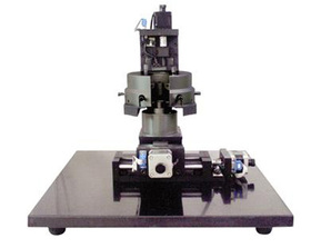
The base:
The base of Atomic Force Microscopes holds the detector, AFM Head. It also has an environmental control attachment along with other optional attachments such as Vibration Isolation System.
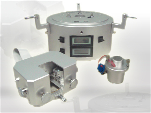
The controller:
The SPM Controller handles all SPM electronics such as signal processing and feedback programming.
The Controller inputs commands from a control computer via 60 pin cable and outputs the control signals that are needed for operating an AFM stage. Additional signals from the stage are relayed through the SPM Controller via the Network cable to the control computer.
At the rear of the Controller, in addition to the Network cable connection, there are two input/output ribbon cables. A 60-pin cable is used to send and receive signals from the microscope stage. A second 50-pin cable is used for accessing all of SPM Controllers signals for testing or experimentation.
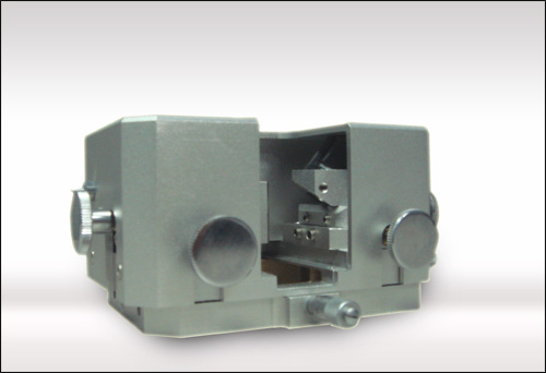
AFM Head holds the following components:
- XY Translation Stage: Holds probe head, movable in XY direction by XY translation screws and in Z direction by controls in software
- Position Sensitive Photo detector (PSPD): Detects laser deflections, which is then converted into a topographical map
- PSPD adjustment screws: controls position of PSPD; screw on left controls up and down adjustment; screw on right controls left right adjustment
- Laser Beam Steering Screws: controls position of laser on back of cantilever
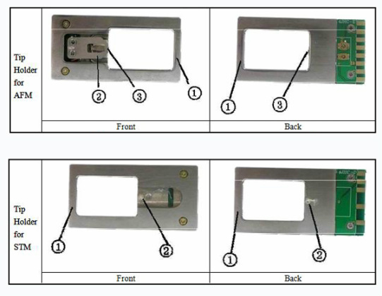
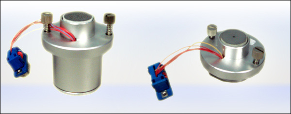
AFM Tipholder:
1 Tip holder Handle
2 Spring Clip which secure the cantilever
3 Cantilever notch
STM Tipholder:
1 Tip holder Handle
2 Installation tube for Pt-Ir or tungsten tips
AFM Contact Mode:
- Topography — the rise and fall of the sample surface.
- Deflection — cantilever flexes because of the rise and fall of sample topography and the amount of this deflection can be reflected by the Photodectetor’s Up-Down signal.
- Friction — lateral forces between tip and sample, which causes the torsion of the cantilever and can be reflected by the Photodectetor’s Left-Right signal.
AFM Tapping Mode:
- Topography — he rise and fall of the sample surface.
- Amplitude — antilever oscillating amplitude changes because of the rise and fall of sample topography.
- Phase — cantilever oscillating phase changes because of the sample material characteristics.
Scanning Tunneling Microscope:
- Topography —the rise and fall of the sample surface.
- Current — Tunneling current changes between tip and sample surface
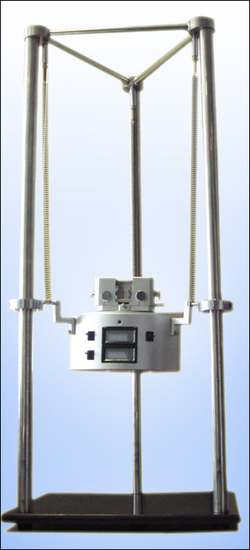
AFM Vibration Isolation System by Angstrom Advanced is made of the highest grade components, minimizing vibration of the Atomic Force Microscope and improving sample quality
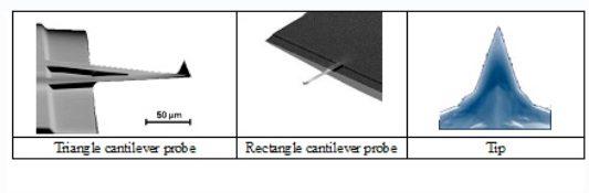
Probes (pictured below):
Different kinds of probes are used in Angstrom Advanced Atomic Force Microscopes. Proper probe selection depends on sample characteristics and system conditions.
Metal Probes
Probe used in STM must be conductive and a atomic-sharp tip is required. STM tips can be obtain by simply cut (for Pt-Ir) and electronically eroded (for tungsten).
Cantilever Probes
A flexible cantilever with an atomic-sharp tip is widely used in AFM as below. Most cantilever probes are made by Si or SiN with different types of coatings and different shape and size.
Different samples and system conditions required different cantilevers.
- Contact Mode: Theoretically all kinds of cantilever probes can be used in contact mode. But because of the different Force constant parameters, harder cantilever will cause the sample damages with the same amount of deflection.
- Tapping Mode: A oscillating cantilever is required in Tapping mode. So theoretically using cantilevers with higher resonance frequency will give better resolution. Cantilevers with larger force constant and higher resonance frequency (normally over 200kHz) should be chosen.
The sample is placed on the Piezo Electric Scanner and is scanned under a stationary cantalever tip (there are AFM models in which the tip is scanned over a stationary sample). The PES is a very precise component and is able to accuratly move the sample through a scan (a back and forth raster pattern) of only a few hundred nanometers. Scanners are made of piezo tubes and are steady held in the SPM base.Voltage applied to piezoelectric scanner tube housed inside moves sample precise increments back and forth. Size at bottom indicates maximum size scan possible,each scanner has its own specified parameters.
Samples are held in place on the scanner with a removable cap. Piezo scanner can extend and retract 3-dimentionally based on the applied X, Y and Z voltage placed across the individual elements.
The feedback system controls the scanner’s Z voltage to maintain the tip-sample force constant, which leads the Up-Down signal equals to the Setpoint. The Z voltage is recorded for calculating the sample topography.
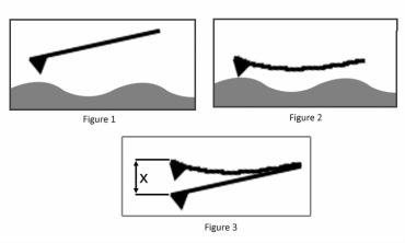
Figure 1: No force between tip and sample, no cantilever deflection.
Figure 2: Repulsion between tip and sample, cantilever deflects upside.
Figure 3: Repulsion between tip and sample, cantilever deflects upside:
X: Deflection of cantilever
k: Force constant of cantilever
F=kx
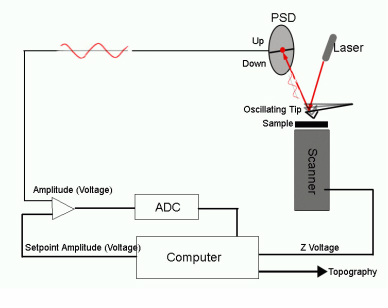
In Tapping Mode, a cantilever is oscillating in free air at its resonant frequency. A piezo stack excites the cantilever’s substrate vertically, causing the tip to bounce up and down. As the cantilever bounces vertically, the reflected laser beam is deflected in a regular pattern over a photodiode array, generating a sinusoidal electronic signal. And this signal is converted to a root mean square (RMS) amplitude value.
When the same cantilever is oscillating at the sample surface, although the piezo stack continues to excite the cantilever’s substrate with the same energy, the tip is deflected in its encounter with the surface. The reflected laser beam reveals information about the vertical height of the sample surface.
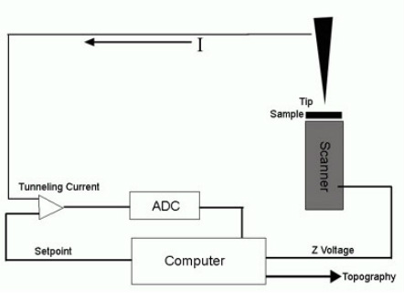
STM relies on “tunneling current” between the probe and the sample to sense the topography of the sample. The STM probe, a sharp metal tip (in the best case, atomically sharp), is positioned a few atomic diameters above a conducting sample which is electrically biased with respect to the tip. At a distance under 1 nanometer, a tunneling current will flow from sample to tip. In operation, the bias voltages typically range from 10 to 1000 mV while the tunneling currents vary from 0.1 to10 nA.
The tunneling current changes exponentially with the tip-sample separation, typically decreasing by a factor of two as the separation is increased 0.2 nm. The exponential relationship between the tip separation and the tunneling current makes the tunneling current an excellent parameter for sensing the tip-to-sample separation. In essence, a reproduction of the sample surface is produced by scanning the tip over the sample surface and sensing the tunneling current.
Angstrom Advanced STM relies on a precise scanning technique to produce very high-resolution, three-dimensional images of sample surfaces. The STM scans the sample surface beneath the tip in a raster pattern while sensing and outputting the tunneling current to the SPM Controller. The digital signal processor (DSP) in the Controller controls the Z position of the Piezo Scanner based on the tunneling current error signal. The STM operates in both “constant height” and “constant current” data modes, depending on the Feedback Gain settings. The DSP always adjusts the height of the tip based on the tunneling current error signal, but if the feedback gains are set extremely low (e.g., Integral Gain < 15 and Proportional Gain < 15), the piezo remains at a nearly constant height while tunneling current data is collected. With the Feedback Gains high (e.g., Integral Gain >15 and Proportional Gain >15), the Scanners Piezo height changes to keep the tunneling current nearly constant, and changes in piezo height are used to construct the image. The exponential relationship between tip-sample separation and tunneling current allows the tip height to be controlled very precisely.
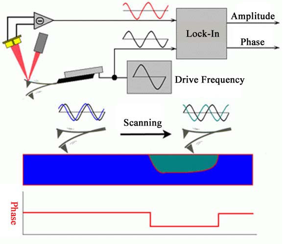
The difference between the actual phase of the oscillating cantilever and the phase of the drive signal can also be detected in Tapping Mode, which is named Phase Mode as shown below:
Phase Mode reveals some characteristics of the sample material itself. These material characteristics may include elasticity ("hardness"), magnetic and/or electric forces present.
Non-Contact AFM Non-Contact AFM oscillates the cantilever at a constant frequency with an amplitude around 10 nm. The height of the surface can be found by measuring the output of the control loop which keeps the frequency constant. Non-contact Atomic Force Microscopes scan much quicker than contact microscopes because the tip does not fatigue. Non-contact AFM is also useful for measuring flexible samples. Contact AFM can scratch and alter the surface of softer samples. The contact method can penetrate through liquids while non-contact will read surface liquids as the sample surface. |
 |
Tapping Method Tapping Atomic Force Microscopes have large oscillations in the tip (100 to 200 nm) which are damped by Van der Waals and dipole forces from the surface of the sample. This method is more gentle than the traditional contact method. The tapping method can also measure through liquid surfaces when used properly. |
 |
Conductive AFM Option (C-AFM) CAFM measures both the surface topography and the conductivity of a samples. Voltage is applied to the tip and the current through the tip and sample is measured. It is used for semiconducting, low and medium conducting materials. |
 |
Contact Mode The tip is always in contact with the sample surface in contact AFM. The deflection of the tip is measured and held constant by a feedback loop. The stiffness of the cantilever must be low enough to prevent the tip from altering the surface of the sample. |
 |
Scanning Tunneling Microscope Scanning Tunneling Microscopes (STM) have a tip which is actuated in the vertical direction by a piezoelectric crystal. The readings from a scanning tunneling microscope are limited by the sharpness of the tip. STM is a different method of getting very similar results to AFM. It maintains a constant distance from the sample through a feedback controller to measure the surface of the sample. |
 |
Angstrom Advanced AFM Options:
Probes:
|
|
Calibration Standards: |
|
Scanners |
|
Optical Microscope System |
|
Vibration Isolation System |
|
Tip Holders |
|


